Summary
The aim of this internship is to realize piezoelectric sensors based on GaN wires, capable of measuring displacement/deformation on a multiscale area (from hundreds of nm to cm) with nm-sensitivity. In the ANR PiezoSens project, different wire-based piezo-sensors architectures will be evaluated in terms of performances and potential industrial applications. This work will focus on the realization of capacitive structures including GaN wires grown by metal-organic vapour phase epitaxy (hundred µm long and ~µm diameter) embedded in a flexible dielectric. This master internship will allow exploring rigid and flexible sensors that will be disruptive with respect to usual piezoelectric devices and explore the physics related to device design, MOVPE growth and technological aspects.
Full description of the subject
Today, laboratory manufacturing enables the realization of piezoelectric devices that are thin, sensitive, mechanically robust & resilient, and in some cases flexible, conformable or even stretchable.
SEM images and EDX mapping of self-assembled InGaN/GaN NWs.
SEM view of GaN wires grown by MOCPE.
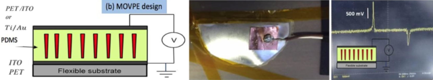
Miniaturized lightweight electromechanical systems going beyond conventional devices are now within the reach of piezoelectric technology. The ambition of the PiezoSens project is to develop piezoelectric sensors based on GaN (nano-)wires (NWs), capable of sensing and spatially mapping displacements/deformations induced by an applied pressure on a surface. A multiscale in-plane resolution will be explored with pressure points from µm to cm in size in (x,y) axes and nm-sensitivity in z (detection of a light touch, 1 kPa). The choice of nitride materials lies in their intrinsic properties (high piezo-response, but also high thermal and chemical stability) enabling bringing materials into real-world devices and providing new novelties in terms of flexibility and functions. The choice of nitride NWs is motivated by their high aspect-ratio conferring to the system beneficial properties in comparison with their bulk & 2D film counterparts: NWs present superior mechanical properties (larger elastic deformation, higher flexibility & resistance), higher sensitivity to applied force, and higher piezoelectric response. For the internship, we propose to take advantage of the specific morphology of the NWs grown by and Metal Organic Vapour Phase Epitaxy (MOVPE) grown in the IRIG, DEPHY department. N-polar GaN wires with a large aspect ratio will be grown and characterized to get a strong flexibility. Due to their rather large diameter, the MOVPE GaN wires will not address extreme resolutions, but their flexibility will be exploited for deformation detection and localization in fully deformable systems: an original use of these materials is to integrate them into a flexible membrane of
polydimethylsiloxane (PDMS) and directly peeled off from the sapphire substrate before metallic electrode deposition. Then, it can be further transferred to a flexible or conformable substrate. The objective of the internship will be to learn the principles of piezoelectricity applied to these materials, to explore some design improvements by the experimental approach, in particular by changing some growth parameters of the wires, the dielectrics and the contacting method. Electrical measurements (output voltage in the volt range) will be recorded as a function of simple mechanical solicitations to validate demonstration devices.
 MBE GaN NWs based design with Ohmic/Schottky electrical collection.
MOVPE GaN wires design with capacitive structure. Note that MBE NWs are a few ~m long, whereas MOCVD wires can reach more than 500 µm lenght.
During the internship, the candidate will interact with the partners of the PiezoSens projects, i.e. CEA Leti/DSYS (for electronics integration, Grenoble) and CNRS/C2N (for nanowires grown by molecular beam epitaxy, Palaiseau) and with the lab researchers working on strain management, characterization and MOVPE growth.
Requested skills
Strong interest in materials science and solid-state physics. Experimental skills to perform nanoscience. Good basis in nanotechnology and solid-state physics.
Keywords
GaN, wires, piezoelectricity, sensors, flexibility
Contact Master/Thesis supervisorJoël Eymery, CEA/IRIG/DEPHI/MEM/NRS, NRS
lab publications Head of CEA "Nanostructures and Synchrotron Radiation” Laboratory
Univ. Grenoble Alpes, IRIG, MEM, NRS, 17 rue des Martyrs, 38054 Grenoble, France.
Phone number: +33 4 38 78 30 15,
joel.eymery@cea.fr