General scope
Long range electric and magnetic fields are present all around us in devices, where electric fields on atomic length scales are present in all matter. However, it remains challenging to measure the strength of these fields accurately and with high spatial resolution. Several Transmission Electron Microscopy (TEM) based techniques exist, sensitive to internal fields. TEM is of particular interest in this respect, since (i) the electron traverses the sample, and can therefore probe all fields it traverses, and (ii) due to the very high spatial resolution that can be obtained in TEM.mprovement of existing software involving IA and neural network.
Research topic and available facilities
The aim of this internship is to contribute to the data treatment of so-called four-dimensional scanning transmission electron microscopy (4D STEM) results. In these experiments, a focused electron probe is raster scanned over the sample, and a diffraction pattern is acquired at each probe position. The presence of an (electric) field in the sample results in a deflection of the transmitted beam. Therefore, careful analysis of the transmitted beam position can give access to electric fields with atomic spatial resolution, and through Poisons equations, to the charge density and electrostatic potential. Different methods exist to extract the position of the transmitted beam, the most commonly used one is referred to as the Center of Mass (COM) approach. The challenge of such data treatment resides in the fact that the beam position is not always very well defined, most importantly because the atoms in the sample may diffract the electron beam. This internship will contribute to data treatment of 4D STEM data obtained on 2- dimensional materials, which are model systems for such studies. The student will integrate a multi-institute, multi- disciplinary research group, including researchers of both CEA Grenoble and CNRS Institut Neel. The student will assist to the 4D STEM experiments and data acquisition on a state of the art double corrected TEM present at the Nano Characterization Platform (PFNC) in Minatec, CEA. Then, the student will analyze different kinds of data sets using the center of mass approach, acquired on different pixelated detectors but on the same sample. A new very fast camera capable of direct electron detection has just been installed at this TEM. The student will compare approaches using already developed scripts and programming in Python and adapt python scripts to the task.
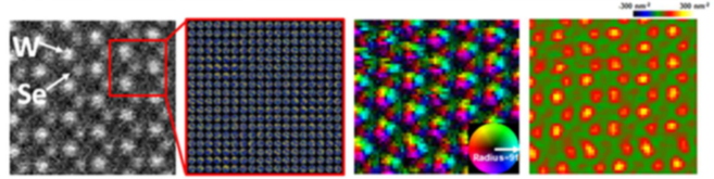
HAADF image of WSe2 monolayer (2D material), local electric field and charge density maps calculated from deflection of transmitted beam.
Possible collaboration and networking
The internship will be in collaboration with Institut Néel (M. den Hertog).
Possible extension as a PhD
Not granted in advance, but we are open to support applications for a PhD grant.
Required skills
Interest in solid-state physics, transmission electron microscopy, interest in programming and data treatment.
Starting date
Jan/Feb 2021 or earlier.
Contact: Hanako Okuno & Martien den Hertog (Institut Néel)
LEMMA/MEM/DEPHY/IRIG
Phone: 0438782073