In the context of the development of photovoltaic technologies, solar cells based on
halogenated hybrid perovskites (HHP) have been the subject of intense studies for the last ten years. These cells are now achieving energy conversion efficiencies close to those of silicon solar cells, around 25.5%. However, many challenges remain to be met in order to match the performance of silicon, particularly with regard to the stability of performance over time, which requires, among other things, control of the structural properties of HHP
thin films. Questions remain, for example, regarding the state of strain and the orientation of the perovskite crystalline lattice.
It is well established that the strain state of the perovskite layer affects its stability, as well as the orientation of the crystalline lattice potentially affects the optoelectronic properties of the perovskite. In an effort to master the
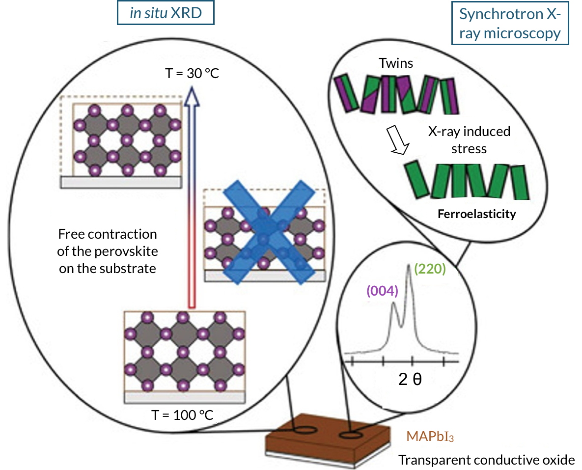
microstructure of HHP thin films, researchers at our laboratory have used laboratory X-ray diffraction (XRD) and synchrotron diffraction X-ray microscopy to identify and understand the mechanisms governing the strain state and crystal orientation of thin films of MAPbI
3, a prototypical HHP compound.
As a first step, we performed
in situ XRD studies to investigate the MAPbI
3 layer strain state. The results lead them to question the commonly accepted assumption according to which HHP films synthesized at 100°C show strain at room temperature due to the difference between the values of the coefficient of thermal expansion (CTE) of the perovskite and the substrate. Our measurements have indeed evidenced, for MAPbI
3 layers obtained with standard protocols, a relaxed (unstrained) behavior of the perovskite film, thus demonstrating the absence of direct correlation between the difference in CTE and the MAPbI
3 strain state.
In a second step, we studied the orientation of the crystalline lattice in these thin films by X-ray diffraction microscopy at the European Synchrotron Radiation Facility (ESRF in Grenoble), which allows to visualize all the crystalline domains with a same given orientation. Our results proved that the double texture sometimes observed in XRD measurements of MAPbI
3 thin films is due to the presence of ferroelastic twins (Image) forming at the cubic-tetragonal structural transition undergone by MAPbI
3 around 57 °C.
 Twin crystals are identical crystals whose orientations are not arbitrary but connected by symmetry operations characteristic of the crystal structure of the material in question.
Finally, these experimental studies have been complemented by density functional theory (DFT) calculations which have shown that the chemical environment at the interface with the substrate ("first layer" of the MAPbI
3 lattice of MAI or PbI
2 type) influences the orientation of the perovskite layer.
These different results constitute an important progress in the understanding of the microstructure of halogenated hybrid perovskite layers, opening the way to the control of their strain state and texture, with the aim of improving their optoelectronic properties, as well as the performance and stability of the devices.
Halogenated hybrid perovskites possess a set of advantageous properties for photovoltaics, rarely present at the same time in other types of materials: a high absorption coefficient, low excitonic effects, a band gap energy allowing good photon collection, good transport properties, high defect tolerance. Moreover, these physical properties can be modulated by chemical engineering, which allows to optimize perovskites to adapt them to the various challenges of photovoltaics such as stability or the realization of multi-junction cells.
The texture of a
thin film characterizes the orientation of the crystal lattice in the direction perpendicular to the plane of the film.
The
microstructure of a crystalline thin film is defined by the strain state, the texture and the coherence length of the crystalline lattice.