The use of strained silicon is a fundamental of modern nano-electronics, allowing to increase the mobility of charge carriers up to 150%. Researchers from INAC (in collaboration with CEA-LETI and ESRF) measured the deformation of individual silicon lines at the nanoscale. With the miniaturization of devices based on semiconductor (in order to increase their efficiency or adjust their properties), the performances have become more dependent of changes within individual structural properties (chemical composition, shape, deformation). It has therefore become necessary to characterize objects through the study of unique objects.
In this experiment, the individual lines of strained silicon (section 225x70nm2) deposited on SiO2 were studied through focused x-ray beam (full width at half maximum of 300x500nm2) on the ID01 line of the ESRF synchrotron. By measuring the diffraction of a single line, it is possible to find the displacement field within the silicon line and hence its deformation.
It was thus possible to follow the evolution of the lines deformation when the intense beam (about 105 photons/(s.nm2)) has altered the interface between silicon and silicon oxide without modifying the crystalline nature of the silicon. A clear relaxation of the line is observed, with a displacement amplitude divided by three. An important point is that despite this relaxation (flattening), the line remains stressed along its main direction, which allows keeping the interesting properties of conduction. Beyond the ability to measure the deformation of a single line, it shows the relative soundness of the use of the axial stress to increase performance in the transistors silicon-on-insulator (SOI) constrained. This study paves the way for the study of the deformation of many semiconductor nanodevices by X-ray diffraction.
Diffraction pattern of a silicon single line.
The curvature in the form of "banana" is the signature of the line of deformation, which can then be reconstructed.
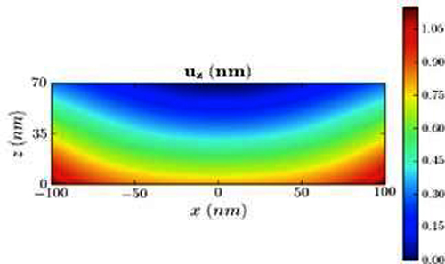
Displacement field reconstructed in the silicon line, with a precision of the order of a few hundredths of nm.