For several years, researchers and engineers around the world have been exploring ways to replace the classic transistor that equips our computers, phones... This replacement should be able to be miniaturized, consume as little as possible and combine several functions. IRIG researchers have been working for many years on magnetic memory architectures that exploit the properties of the electron's spin when it crosses a ferromagnetic layer. In collaboration with researchers from the CNRS/Thales laboratory at Orsay, they have just taken an important step to demonstrate the applicability of new architectural concepts that could be good candidates.
In some materials, the orientation of the electron spin is related to the direction along which it propagates. An electron passing through a ferromagnetic layer has its spin oriented according to the local magnetization. The current is then called spin polarized. A spin current injected in one direction can create a charge current in another direction of space. It Is the so-called spin-charge conversion, that needs to be maximized in these new architectures. The elementary brick necessary to obtain interconversion must be a stack composed of a ferromagnetic layer whose purpose is to polarize the spins, and a second layer in which interconversion takes place.
We found that the optimal system was a multi-layer stack, SrTiO
3\Al\NiFe where SrTiO
3 (STO) is an oxide that conducts currents very poorly, and NiFe is a ferromagnetic material that provides the source of polarized spins. The thin layer of aluminum, at the interface and in contact with the STO layer, creates a very good electron propagation layer in the form of a two-dimensional electron gas (2DEG). It is in this gas that the interconversion takes place. Using various imaging and spectroscopy techniques of transmission electron microscopy, researchers were able to measure the atomic scale reduction of STO at the interface with aluminum, and explain the creation of the two-dimensional electron gas 2DEG (
Figure).
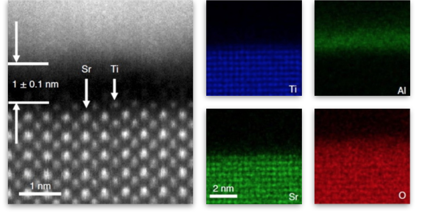
On the left: Electron microscopy image of the STO\Al stack (9Å). On the right chemical maps showing that oxygen has diffused following the deposition of aluminum.
The spin charge conversion was six times higher in this type of stacking. These results indicate that 2DEG oxides are strong candidates for spin-based information reading in new memory and transistor designs.