Contact:
Jean-Luc Rouvière Overview
 Electron Diffraction Maps (eDM) generally denominated 4D-STEM experiments, are full of interesting pieces of information. The LEMMA group has been developing such approach for Strain field measurement for more than 15 years (read this
short overview and
Strain characterisation at nanoscale using Transmission Electron Beam Based techniques). Initially, scanning and acquisition were performed by scripting in Digital Micrograph (a software sold by the Gatan company) and the scanning and acquisition were rather slow (about 0.5 s per diffraction patterns, so it could take more than one hour to acquire an eDM). Rather recent developments in software and hardware, especially new direct electron detectors, have been boosting this eDM approach. Presently, the LEMMA group pushes more and more this eDM approach to determine electric and magnetic potential fields at nanometer or atomic scale.
eDM for strain measurement (coll. LETI, ST-microelectronics, IBM, Prof. Zuo J-M, FEI)
LEMMA has used and partly improved many electron microscopy sub-techniques to determine strain in nanostructures at either a nanometric and atomistic resolution.
The table 1 of this short review paper gives a list of these techniques.
For applications, Nanobeam Precession Electron Diffraction (N-PED) is presently the more interesting and used techniques. Thanks to our developed software (Mk_Precession_II, acquisition software developed by and in collaboration with FEI, now TFS and GEM_ED, a LEMMA digital micrograph script), 2D-strain maps of many nanostructures – especially on microelectronics devices - are routinely acquired (see Figure 1).
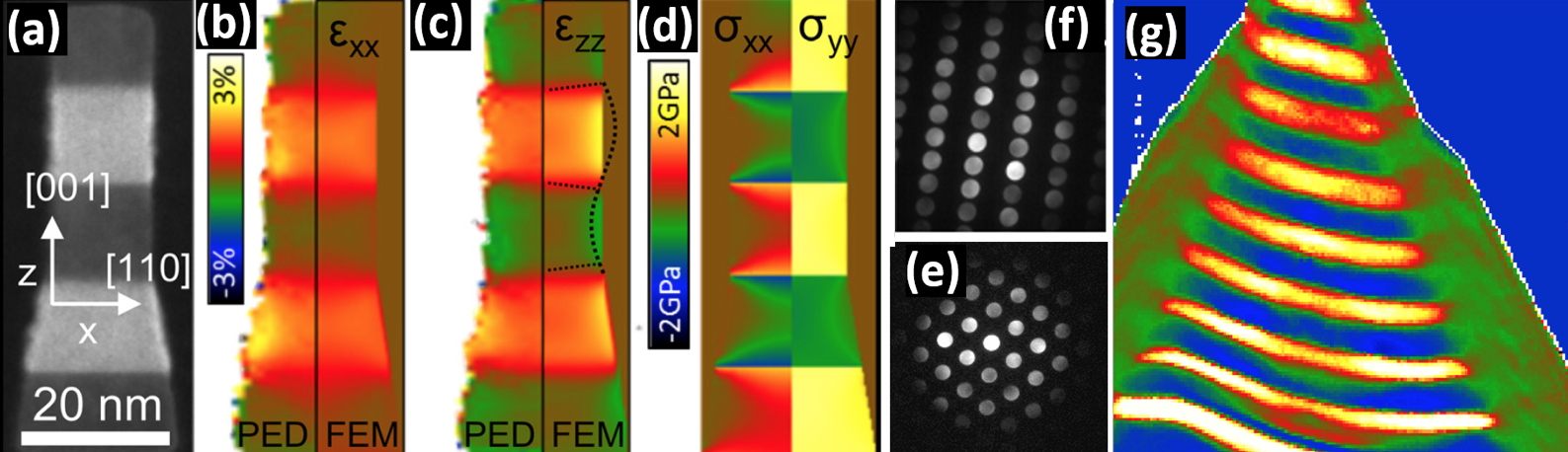 Figure 1: (a) Dark Field image of the FINFET device. (b)-(c)-(d) strain and shear in the device image as determined experimentally (PED on left) or calculated by Finite Element Modelisation (FEM on right) (e) Typical local Precession Electron Diffraction (PED) pattern in Si. (f) One PED pattern extracted from the eDM that has been acquired in a sample containing AlN/GaN multilayers (f) Experimental strain map (along the growth direction) obtained in a pyramidal nitride Nanowire containing AlN/GaN multilayers. GaN layers appears in yellow because they have a larger lattice parameter than AlN (in blue in this strain map).eDM for electric and magnetic fields with nanometer spatial resolution
 (coll. LETI, INEEL, Nanomegas)
eDM is an emerging technique for measuring electric and magnetic fields at a nanometric or atomistic scales. In the past, essentially in collaboration with CEA-LETI, LEMMA has tested other TEM techniques, like holography and iDPC to measure these fields (
for instance).
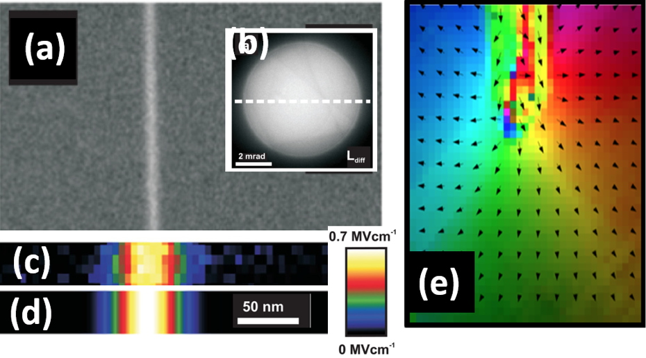
Presently, thanks to the installation in 2021 of a MERLIN direct electron Detector on an advanced double-corrected TITAN microscope, we got some very interesting and promising results in electric fields in pn-junctions and magnetic nanowires (Figure 2 and publications) and
more recently in 2D-materials. Thanks to collaborations with INEEL and CEA-LETI, evolution of charge distribution with applied voltage can be measured
in-situ in the microscope. As for
Strain Measurements, we found that the use of Precession can improve the precision of the electromagnetic fields measurements and a patent has been deposited to valorize these findings (
Patent 20180076005)
eDM for atomic structure determination (coll. INEEL - France, Jülich - Germany, Berlin - Germany)
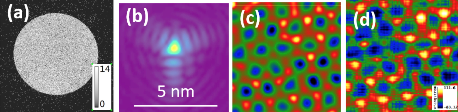 Figure 3. A simple comparison of the ptychography and COM approach on experimental eDM data obtained at PFNC on the TITAN Ultimate microscope. The studied sample is MoS2 2D-layer. (a) Average of all the diffraction experimental diffraction patterns of the eDM: camera length has been chosen in order to focus on the direct transmitted beam (the large white disk with noise of the figure). (b) Intensity map of the incident electron probe has determined by a ptychography reconstruction. (c) Ptychography reconstructed atomic potential of the MoS2 layer. (d) COM-reconstructed atomic potential of the MoS2 layer.
LEMMA is presently exploring 2 approaches for obtaining high resolution images that is say images where atomic columns or individual atoms can be resolved. One approach, is the use of the
Center of Mass (COM) method to determine the projected electric field (Figure 3d). The second approach is to inverse numerically the Schrodinger’s equation that describes the propagation of electrons within the sample. This second approach which is generally called ptychography (Figure 3b and c) is of course more powerful and accurate than the COM approach: ptychography can reconstruct (i) the electron wave function in different planes and in particular the incident wave function (Figure 3b) (ii) but also the interaction potentials projected on different slices (in Figure 3c only one slice has been used) and the obtained potential map is smoother than the COM one (compare Figure 3 c and d). As shown in Figure 3, reconstructed ptychography and COM potentials are very similar in 2D-materials and we are trying to understand their differences and why COM works so well in spite of its simplicity. By the end of year 2023, we should have post-doc positions for these topics or some linked one. This post-doc positions
will be advertised here.