Contact:
Hanako Okuno
LEMMA laboratory is developing advanced microscopy techniques to study low-dimensional materials including 1D- and 2D-materials and atomically thin interfaces. To avoid the beam irradiation damages, generally low-voltage aberration corrected (S)TEM is used for material analysis. The main purpose is to provide structural and chemical information at atomic scale with our expertise in monochromated TEM, aberration corrected STEM, EDX, EELS and 4D-STEM using two state of the arts microscopes (Titan Ultimate and Titan Themis). We are working on diverse problematics in low-dimensional materials, such as growth and property control, in strong national and international collaborations with several research groups.
Main collaborations :
Spintec, L_Sim, Leti, LTM (CNRS), Institut Néel (CRS), IRAMIS (CEA-Saclay), NCSR (Greece), UCL (Belgique)
 Structural analysis of graphene (coll. Liten, L-Sim, Institut Néel, INP, IRAMIS)
Structural defects are considered as a parameter-tuning knob for tailoring physical properties of 2D materials. The ability to engineer atomic defects at nanometer scale opens up unique opportunities to alter and enhance electrical, optical, mechanical and magnetic properties. Despite the growing interest in 2D materials, growing defect-free 2D materials on desired substrates remains a challenge. Identification and characterization of these inevitable intrinsic growth defects are thus an essential process. As graphene is one-atom thick layer consisting of only light carbon atoms, atomic structure analysis requires a special microscopy condition. Titan Ultimate equipped with image aberration corrector and monochromator allows to achive atomic resolution TEM imaging at 80kV and provides information on atomic defect structures to study the growth and properties.
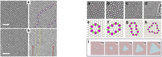
Figures: (left) Grain boundary with 5-7 lines defects and dislocations found in CVD graphene, demonstrated as the key for re-crystallization (A. Tyurnina et al.,Carbon 102 p499, 2016) and (right) experimentally observed flower defects and related DFT calculated structures, which are used for “engineering by design” concept (A. Cresti et al., Carbon 161 p259, 2020).
Epitaxilly grown TMDs and their VdW heterstructures (coll. Spintec, NCSR, LTM)
Atomic structures in MBE grown transition metal dichalcogenides (TMDs) and related materials can be identified using monochromated TEM and aberration corrected STEM (Titan Ultimate and Themis). HAADF Z-contrast imaging provides local atomic position together with their elemental attribution. VdW and quasi vdW epitaxial growth is studied by either plan-view or cross sectional analysis, providing information on local structural correlation between stacked materials. Newly developed 4D-STEM imaging enables to map local orientation and phase in epitaxially grown 2D monolayers. These techniques are combined with other analytical techniques (XRD, AFM, XPS, STM) to study growth mechanisms and to explore new functionality of materials in strong collaboration with materials teams.
In situ observation (under e- irradiation and/or at high temperature) is also used to study the dynamics of structural modification.

Figures: (left) Typical defect found in MBE grown MoSe2 determined by monochromated TEM imaging. Inversion domains are formed due to Se deficiency induced during the growth process (C. Alvarez et al., Nanotechnology 29 p425706, 2018) and (right) Cross sectional STEM image of Fe5GeTe2; complex Fe atom position was determined by a comparison with simulated image (M. Ribeiro et al., 2D Materials and Applications 6, p1, 2022).
Chemical analysis of atomically thin layers
Local chemical identification in 2D layers can be achieved by two different techniques. HAADF Z-contrast imaging gives a quantitative chemical contrast. Impurities as dopant and/or elements in heterostructures are locally determined by comparing the intensity profiles in experimental images and simulated ones. As the intensity profile is sensitively impacted by residual aberration and sample tilt, a perfect microscopy setting is required for reliable chemical analysis. EELS spectroscopy is also used for direct elemental determination. However the technique requires a long acquisition time to correct enough signals, special sample preparation is often needed, such as extreme clean surface and/or graphene protection layer, for damage free analysis at 80kV.
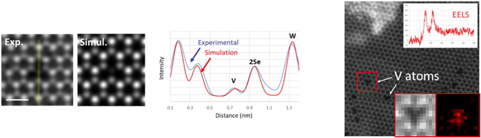
Figures: Identification of vanadium single atom dopant substitutionally integrated in W site of WSe2 monolayer (P. Mallet et al., Physical Review Letters, 125, p036802, 2020) by different microscopy techniques; (left) Z-contrast quantitative imaging and (right) EELS atomic resolution spectrum imaging.
Atomic scale electric field mapping by CoM (coll. Institut Néel, UC Louvain)
We are currently developing diverse 4D-STEM techniques in the laboratory (See also). A focused electron probe is raster scanned over the sample, and a diffraction pattern is acquired at each probe position. The presence of an (electric) field in the sample results in a deflection of the transmitted beam. Therefore, careful analysis of the transmitted beam position can give access to electric fields with atomic spatial resolution, and through Poisons equations, to the charge density and electrostatic potential. Using low voltage aberration corrected STEM and a high speed camera, electric field in 2D monolayer can be mapped by measuring the Centre of Mass (CoM) in transmitted beam. The technique is under development for the purpose to investigate defect induced local charges in 2D materials, such as doped or Moiré samples.
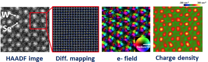
Figures: HAADF image of WSe2 monolayer (2D material), local electric field and charge density maps calculated from deflection of transmitted beam (ongoing PhD Thesis of K. Sharma and D. Desenovic).
Interface analysis (coll. NPSC, LTM, Spintec)
Cross-sectional specimen prepared by FIB technology allows access to interface analysis of stacked building blocks such as thin layers and vdW heterostructures. Study of phenomena happening at atomic interface, such as intermixing, diffusion, intercalation, evolution of chemical bonding state, is possible by combining (S)TEM imaging and spectroscopy.
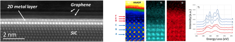
Figures: (left) 2D indium metal layer formed under graphene layer via intercalation between buffer layer and SiC substrate (N. Feldberg et al., Nanotechnology 30, p375602, 2019) and (right) evolution of oxidation state of Ti in extreme surface of STO at the interface with Al, followed by EELS spectrum imaging (DC Vaz et al., Nature Materials 18, p1187, 2019).