The use of Gallium nitride (GaN) compound semiconductors has recently become very popular in visible optoelectronics to obtain blue and white light sources. Current technologies for solid-state lighting or LCD screen backlighting are based on planar growth of InGaN/GaN quantum wells. The indium composition and the thicknesses are controlled so as to choose the emitted color. Blue light is obtained quite easily, while green and yellow emitters are more difficult to master.
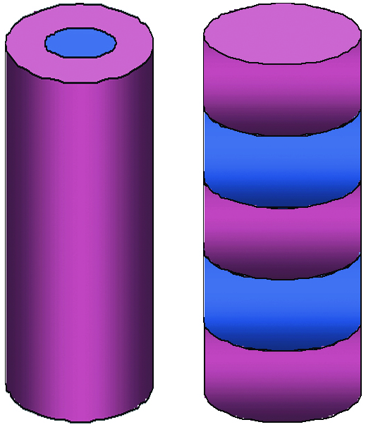
Figure 1: Radial and longitudinal heterostructures in nanowires.
The use of GaN wires brings several important advantages. The light extraction efficiency is increased due to a larger free surface area. Their structural quality and hence their optical properties are much less affected by a lattice parameter mismatch with the substrate than equivalent planar layers. Longitudinal or radial heterostructures can be grown (Figure 1) that take advantage of the elastic relaxation properties at free surfaces in nanowires. Finally, the integration of wire-like objects is of interest both for electrical devices by simplifying the contacting and the definition of the doped zones and for optoelectronics devices for which an adaptation of the wire diameter provides efficient waveguiding of the light along the wire.
Our laboratory has had a precursor role in France in the last few years by developing the growth of nitride semiconductor-based wires by metal-organic vapor phase epitaxy. This research has led to some surprising results. In the simplest case of GaN homoepitaxy, it is possible to choose the growth morphology either as wires (Figure 2 a) or as pyramids (Figure 2 b) by changing the polarity of the substrate (Figure 1), i.e. by flipping it upside-down!
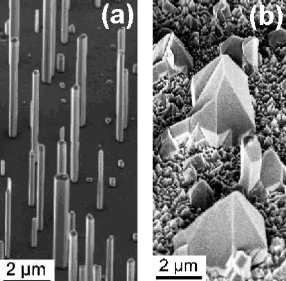
Figure 2: Influence of the substrate polarity on the crystal morphologies. For the same growth conditions through a thin Si3N4 layer deposited on a GaN substrate, the result is either (a) -c oriented wires or (b) +c oriented pyramids (see the inset for the definition of the axes).
Both these morphologies are used to grow heterostructures. For wires, (Figure 3 a,b) the lateral surface covered by InGaN/GaN quantum wells is controlled by the growth conditions. In this case, the growth is on non-polar surfaces (the lateral facets of the wire) so that contrarily to growth along the c-axis of the crystal (in that case the wire’s long axis), there is no local electric field to induce a spontaneous spatial separation of electrons and holes. For pyramids, whose section is controlled by the Si3N4 mask and a selective growth, quantum dots can be grown at the tip (Figure 3 c,d). The regularity of these objects determines precisely their emission properties.
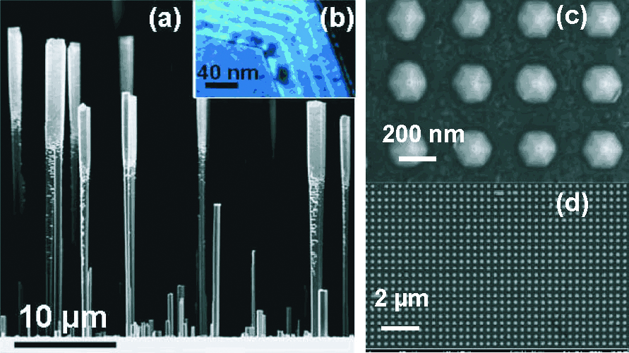
Figure 3: Multiple InGaN quantum wells (around 16% indium) on GaN wires. The wires are oriented along -c (see figure 1) and are observed
a) from the side in scanning electron microscopy and
b) in cross-section in transmission electron microscopy. (c-d) Views from the top of +c oriented pyramids (see figure 1) with InGaN quantum dots grown at their apex.
Heterostructures based on wires have already been used in collaboration with Institut d’Électronique Fondamentale (Orsay) to make photodetectors and emitters based on horizontal wires. In this case, wires are cut in an ultrasonic aqueous bath, dispersed on a host substrate and electrically contacted. Similar growths of radial heterostructures on Si substrates covered by a thin polar AlN buffer are currently being investigated in collaboration with Institut LETI. In this case, the wires stay vertical and are contacted directly through the substrate, which facilitates their integration in devices.
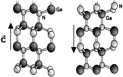 Polarity
 Two views of the wurtzite structure of GaN, with opposite polarities. The +c axis that links the cation to the anion is a polar axis, meaning that one of its ends cannot be linked to the opposite end by a symmetry transformation of the crystal. This property results from the absence of inversion symmetry along the growth axis.